Friday August 27th - Pixel and Delay scaning
There is a LOT of data taken here so when ive entered it ill post a link
Thursday August 26th - Characterising Laser Pulse and FirstPixel scans
pulses of different lengths and amplitudes were sned to te laser (which was aimed at the test bit) and the reaction of the test bit's shaper was noted. The pulses were sent in pairs 200ns apart
| pulse to laser | shaper response |
| 1ns , 1.2V | 1mV |
| 2ns , 1.2V | 3.4mV |
| 3ns , 1.2V | 10mV |
| 4ns , 1.2V | 20mV |
| 5ns , 1.2V | 48mV |
| 6ns , 1.2V | 107mV |
| 7ns , 1.2V | 147mV |
| 8ns , 1.2V | 150mV |
| 9ns , 1.2V | saturates 223mV |
| 10ns , 1.2V | saturates 223mV |
| 9ns , 590mV | 9.6mV |
| 10ns , 590mV | 10.8mV |
| 9ns , 800mV | 26.8mV |
| 10ns , 800mV | 32mV |
| 9ns , 1.05V | 64mV |
| 10ns , 1.05V | 112mV (4mv of undershoot) |
| 9ns , 1.1V | 116mV |
| 10ns , 1.1V | 220mV saturating |
| 3ns , 1.3V | 14mV |
| 4ns , 1.3V | 191mV |
| 3ns , 1.25V | 12.4mV |
| 4ns , 1.25V | 34mV |
| 5ns , 1.25V | 225mV |
| 4ns , 1.21V | 24mV |
| 5ns , 1.21V | 60mV |
using this 60 mv shaper pulse (mening its roughly equivalent to a 5000 electron pulse) some scans across pixels were taken. to determine teh spot size by the rise time as the pixel turned on the results are here
a scan using single 5000 electron equivalent pulses (now a 950mv pulse to the laser with the new spot sixe) to measure the efficiency as a function of a delay from the trigger
| delay (ns) | efficiency |
| 1 | 100% |
| 2 | 100% |
| 3 | 98.5% |
| 4 | 91.8% |
| 5 | 72.4% |
| 6 | 39.8% |
| 7 | 13.8% |
| 8 | 4.03% |
| 10 | 0.11% |
| 15 | 0% |
NOTE - we ned to set the delay controll to 7, the misc_controll to 192 and teh test_pixel_fine dealy to 26
Wednesday August 25th - Took first optical data
Today we finally got the fibre mounted over the assembly (#6) applied a 5ns long laser pulse and read out the text pixel. Weare able to move it with good precisionm at least tenths of mm probaly micron in X (along a row), Y(up and down a column) and Z(above and below).
The fiber end was moxed into the following piostion over the test pixel x=3.00mm y = 3.835nn, z=2.73mm.
| voltage of 5ns pulse applied to laser | shaper output from test pixel |
| 1.0V | 10mV peak |
| 1.1V | 26mV peak |
| 1.2V | 63mV peak |
Tuesday August 24th - Final Electronics Measurments and preperations of optical pulsing
-re took a seriesof electrical measurments with VTH set to 213 to make the threshold approximatly equal to 1,800 electrons. So the amplitude produced by teh opulser will eba ctually 50 mV.
| Shaper Trace | Discriminator Trace | ||||
| Pulse Name | Total Width | Peak Seperation | Total Width | Rising Edge | Falling Edge |
| 505025 | 55.2ns | - | 91.34ns | - | - |
| 505050 | 81ns | 39.3ns | 112ns | - | - |
| 505075 | 96ns | 57ns | 125ns | - | - |
| 505080 | 144ns | 64ns | 143ns | - | - |
| 505085 | 160ns | 81ns | 146ns | - | - |
| 505090 | 162ns | 84ns | 148ns | - | - |
| 505095 | 163ns | 78ns | 152ns | 63ns | 88ns |
| 5050100 | 187ns | 96ns | 172ns | 65ns | 92ns |
Then for the same series of traces the delay fromr the trigger , measuring teh rising edge of teh shaper and discriminator pulses.
| Pulse | Shaper | discriminator |
| 505025 | 93ns | 114ns |
| 505050 | 100ns | 135ns |
| 505075 | 94ns | 133ns |
| 505080 | 95ns | 135ns |
| 505085 | 95ns | 132ns |
| 505090 | 93ns | 134ns |
| 505095 | 93ns | 136ns |
| 5050100 | 94ns | 132ns |
Now we changed to a chip with a sensor designated asembly 6. Applying 80V silicon bis to stop teh sensor capacitane from massivly ioncreasing teh noise compared to the unbonded read out chip.
A scan was made of VTH = 207 to VTH = 215 . This placed the value thatmade the threshold 1,800 electrons at 207.
Now using teh INTERNAL pulser and trigger (so a square electrical pulse) measurments to investigate timewalk were made
| Pulse Amplitude | Shaper Peak | discriminator edge | VTH | |
| from trig | height | |||
| 100mV | 92ns | 120mV | 92ns | 216 |
| 90mV | 91ns | 110mV | 91ns | 213 |
| 80mV | 91ns | 100mV | 91ns | 213 |
| 70mV | 91ns | 90mV | 91ns | 213 |
| 60mV | 91ns | 78mV | 91ns | 213 |
| 50mV | 91ns | 67mV | 91ns | 213 |
| 40mV | 91ns | 53mV | 95ns | 213 |
| 35mV | 91ns | 50mV | 95ns | 213 |
| 30mV | 91ns | 40mV | 99ns | 213 |
| 25mV | 91ns | 32mV | 99ns | 213 |
| 20mV | 91ns | 26mV | 102ns | 213 |
| 18mV | 91ns | 22mV | 103ns | 213 |
| 16mV | 91ns | 20mV | 106ns | 213 |
| 15mV | 91ns | 19mV | 106ns | 213 |
| 10mV | 91ns | 12mV | - | 213 |
| 8mV | 91ns | 9mV | - | 213 |
| 5mV | 91ns | 4mV | - | 213 |
| pulse | Shaper Delay | Disc delay | Disc Amp | VTH |
| 18mV | 91ns | 107ns | 640mV | 209 |
| 16mV | 91ns | 106ns | 520mV | 209 |
| 50mV | 91ns | 93ns | 1V | 209 |
The calculation above giving teh VTH as 207 was done and some efficiency measuements were taken with all the bits other then the test bit masked
| Pulse amp | efficiency |
| 10mV | 0% |
| 16mV | 4% |
| 18mV | 28% |
| 19mV | 50% |
| 20mV | 72% |
| 50mV | 100% |
| VTH set to 208 | |
| 10mV | 0% |
| 16mV | 7% |
| 18mV | 38% |
| 19mV | 62% |
| 50mV | 100% |
| VTH set to 209 | |
| 10mV | 0% |
| 16mV | 12% |
| 18mV | 15%,51% |
| 19mV | 75% |
| 50mV | 100% |
Another VTH scan was done now with the masking ON to see if the 207 209 descrepancy could be resolved. This Also produced a 207 result. Another was then done with MUCH higher statistics (1000 triuggers per point) and it came out at 209.
The fiber mounting system was nearly completed. Optical testing should begin soon
VTH Scan monday 23nd August
In order to match teh simulations it was neceary to scan through a series of VTH values to find which coresponded to 1800 electrond. The results are here in an excel document.
Thierry Gys should be able to provide a mount for the laser's fiber tomorrow so hopefully the light pulsing should be abel to begin soon.
Weekend 21st 22nd August
began rewriting wafer testing code
Continuing Backpulse Measurments - Friday 20th August
The threshold scan taken yesterday indicated that the threshold was approximatly 1000 electrons. The simulaiton was origionally made assumng this to be 1800 electrons. To rescale for this the pulses had to be reduced fomr 50mv to 27.8mv. This meant that the ampllitude of the pulser had to be set to 111mv and not to 200mv sa it was previously - luckily this did not require any reprogramming of the puse shapes.
A series of traces were labouriuosly recorded ontol floppy diskusiong the scope. For each pulse setting 4 sets of 2 (overlapping) traces were taken. (the zipped result file for the 50mv scans is here)
- Pulse shape - The twopulsestake herer are oe from teh inverted channel of the pulser and one from where its injected into the board
- Shaper - The output from the test pixel shaper, and the input from the pulser seen above.
- Analouge Discriminator - the shaper and a probe on the analouge discriminator
- Synchroniser - A probe on teh synchroniser and the analouge discriminator
these were taken for each of the dual 50mv staircases - 505025, 505050, 505075, 505080, 505085, 505090, 505095, 5050100. These refer to two 50mv staircases with a (for example 75ns shelf in between.
Getting a laser pulser and taking initial backpulse measurements - Thursday 19th August
A 1066 laser pulser that should have the required charavcteistics (fast rise time and repeatpulse) has been borrowed, along with a fibre that will focus light down to a 10um spot 12mm from the end of the fibre. These will be connected to the pulse generator we already have.
A long threshold scan was made of the test pixel. Normally these make 40 meaurments this took 10,000 and took most of the afternoon. I also edited the pulse files again to only have a 10ns lead time not 50ns. I didnt startr taking the other sets of measurmetns because i noticed that the inverted signal coming from the pulser seemed to be higher then it should have been and so decided to wait untill tomorrow when Ken or Alex could have a look at ti and make sure that ther is nothing seriously worng.
The results from the threshold scan will be uploded when i have them off the lab computer.
Pulsing the Test Circuit - Wednesday 18th August at CERN
The pulses produced by the pulser (aka the arbitary waveform generator) were applied to a packaged assembly mounted on a test board. Normally when the test pulse is applied it is done using an internal characteristic of the board where two lines at different voltages are rapidly switched between on the chip. To get the double pulse "staircase" shape that we need the swich (which is on teh pixel itself) is set to one of these lines and the pulse sent along this line. The problem with this is mainly that the board and chip werbt designed to operate in this more and so we are trying to drive a fast pulse into a reasonably high capacitance. Initally no signal was getting through at all - this was solved when the capacitors on the baord (4.7 micro-farad) that were designed to keep the voltages where they were set were removed. Unfortunatly ther is still come capacitance in teh chip itself that provides an intrinisc limit to how fast a signal can be driven into it.
This capacitance is made up ofeach column having a 3pf capacitance and a parasitic capacitance of about 30pf (+/- 10%). There is approximatly another 10pf for the test board tracks. This leaves us with an approximatly 140pf over all giving a 10ns time constant. We spent the rest of the day characterising this by measuring the actual pulses that were driven intot he system fomr the pulser. Thee can then be simulated so that the simulations results can be checked.
Two series of staircase pulses were made and were characterised by the duration and height of the first step - the second was always long and 50ns high.
| pulse linked to CSV result file |
| 50mv 25ns |
| 50mv 50ns |
| 50mv 75ns |
| 50mv 80ns |
| 50mv 100ns |
| 16mv 25ns |
| 16mv 50ns |
| 16mv 75ns |
| 16mv 100ns |
These wil now be fed into the simulation of the chip to allow us to compare the results ft eh simulation with the effectof applying these pulses. Obvioulsy the 10ns time constant has significantly reduced the usefulnes of teh measurments that can be taken using electronics alone so it is now importantr to get thee measuerments done quickly and begin taking measurements with an optical pulse that isnt affected by the time constant
Setting up Programable pulser - Tuesday 17th August at CERN
Today was spent setting up a series of pulses to apply to a packaged assembly with Alex Howard. These were programmed intoa sony/tektronix programable pulser. This allwas you to enter arbitraty pulse shapes in a number of ways from a binary number representing teh voltage requitred at every nanosecond to a series of equations and a graphical interface. We chose to enter the step shapes we wanted to use as equations / code. These had to be in the following form:
range(0.0,50ns)0.9
range(50ns,75ns)
0.95
range(75ns,1us)
1.0
A series of these pulse shapes were stored in the generators interanl memory. Then the connector to the normal pulse from teh board to the chip mouitng board was cut, and the pulse generator connected, it was then set top be triggered from the controller board. We have had some difficulty gettingit to work past this point and probaly need the assistance of ken who will be back tomorrow.
Assembly Testing - Monday 16th August at CERN
This is a quick write up of todays activities and their results. Ken Wyllie and I spent most of the day testing 5 assemblies produced by VTT. These were slightly different because they incorporated an extra Titanium Tungsten layer to prevent the de lamination problem described earlier. VTT had some trouble producing them and the fact that they sat on the shelf for a few months after the solder had first been re flowed may have had something to do with it. In the end to make the bump bonding process work they had to re-refolw the solder and bump bond them. Of the ten produced in this manner half were tested at VTT and half were sent to CERN.
The tests performed consisted of:
- Checking the voltages and currents supplied and drawn from the MB and Franscoise boards.
- Checking the JTAG connections. An interface to the chip.
- Reading out the assembly with a small silicon bias applied and using the internal pulses
- Reading out the assembly with the bias applied and using a strontium source to provide hits
- Performing a 'Voltage Scan' where different biases are applied to the silicon, and its current measured usually in t he range of tens to hundreds of nano Amps
In addition to the extra reflow, assemblies 2 to 5 had an extra 300 degree centigrade bake out for 180 minutes to simulate the bake out they would experience in the HPD manufacture process.
Assembly #1
In this assembly the initial chip currents were very high. It looks like It was damaged beyond reclamation by the process.Assembly #2
The chip currents and JTAG check were passed, but when the pixels were scanned there appeared to be two dead areas, one each at the top and bottom right hand corners. These were also seen when the strontium, source was used to scan the pixels.
The VTH value of this chip was 204| Silicon bias | Current |
|---|---|
| 100V | 84nA |
| 90V | 80nA |
| 80V | 77nA |
| 70V | 73nA |
| 60V | 70nA |
| 50V | 67nA |
| 40V | 64nA |
| 30V | 60nA |
| 20V | 54nA |
| 10V | 41nA |
| 5V | 14nA |
Assembly #3
The chip current and the JTAG were fine, the fast scan was ok except for a small inefficient region in the bottom right corner. This disappeared in the strontium scan indicating that it was an inefficient area rather then a totally dead one.
The VTH was 206, and after a million strontium triggers 8070 pixels were fired| Silicon bias | Current |
|---|---|
| 100V | 360nA |
| 90V | 367nA |
| 80V | 328nA |
| 70V | 285nA |
| 60V | 214nA |
| 50V | 171nA |
| 40V | 127nA |
| 30V | 86nA |
| 20V | 64nA |
| 10V | 49nA |
| 5V | 20nA |
Assembly #4
In this assembly the analogue current was very low (180mA), no back pulse data could be taken only noise. From this we assumed that the chip was dead.Assembly #5
The chip currents were within bounds, the JTAG and fast pixel scan were ok (the pixel scan looked very clean).
The VTH value was 204 and there were 8109 hits after a million triggers with the strontium source.
| Silicon bias | Current |
|---|---|
| 100V | 117nA |
| 90V | 111nA |
| 80V | 100nA |
| 70V | 90nA |
| 60V | 78nA |
| 50V | 69nA |
| 40V | 61nA |
| 30V | 57nA |
| 20V | 53nA |
| 10V | 35nA |
| 5V | 13nA |
The procedures for handling and testing
The assemblies are held in a gel pack (which releases them when vacuum is applied to its underside) and picked up by a suction pen. Then are vacuumed onto the jig that is itself vacuum held to the 8" wafer chuck on the Suss-microtek probe station. The chuck is moved into the align position (500micons below contact) and the chuck is rotated and translated so that the pins of the probe card match the test pads. Contact is made and then unmade and the pads checked for scratch marks that indicate a good contact is made. The assemblies are then bout back into contact and the silicon bias needle is touched onto the aluminium strip around the edge of the sensor chip. This applies the silicon bias to the sensor chip. The tests detailed above are carried out (with a light shield in place) and then the chuck is set to the load position, the vacuum turned off and the assembly changed for another one.
Trip to VTT in Helsinki - 07-06-04 to 10-06-04
Ken Wyllie and I travelled to Helsinki to set up an assembly probe station/test system for the LHCb HPD assemblies which are being processed there.
The first step was to move the extra equipment required to test the assemblies into the clean room. There was already a Karl-Suss probe station of the same model as the one used in the CERN clean room available so this equipment comprised the MB and F boards, a controller PC running windows XP and Labview, a power supply box, the probe card, a board with a test chip mounted on it and a selection of cables to connect all these components together. These were all thoroughly cleaned with water and propanol and high pressure nitrogen.
The two boards (for reasons of cable length and convenience) were mounted on an aluminium plate inside the light tight box that surrounds the probe station, with the PC and Power supplies outside the box. The power lines, lemo, Jatag and S-link cables all exited through a port a the back of the light tight box.
We were able to successfully contact the test Chip and run a 'fast scan', check its Jatag connection and perform a DAC scan. This indicated that the Electronics of the test system was working reasonably well and was installed properly. Unfortunately due to problems with the probe station itself and a lack of completed assemblies we were unable to test the probe card.
The problems with the probe station were that the computer controlling it was unable to move the chuck in either software mode or with the joystick panel. This seemed to be because of either a problem with the way it was configured or a hardware fault in the probers interface cards that communicated with the PC via a serial cable. We spent the majority of our time at VTT trying to make this work.
The reason that there were no assemblies to test was due to a problem with the 5" sensor wafers. The problem is that the photo resist which is 'spun' onto the metalised surface of the wafer, to give it an even, set thickness, and then baked to harden it was detaching itself during the development phase. To try and solve this a new bottle of the photo resist was attached to the machine, and a variety of baking times were tried - all with only limited success.
Friday, February 27th, 2004 Electronics - workng with Ken Wyllie on the HPD test System
This morning, afternoon and yesterday afternoon, i spent several hours working with Ken, learning about the HPD test electronics.
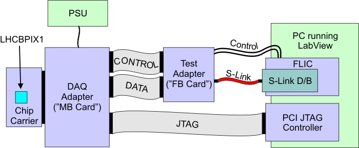
the set up has several parts and is connected as detailed below
- PC (running labview) has a scusi card and a pci card with an rj45 (but not ethernet - Slink) daughterboard and 2 lemo connectors (this PCI card is the flic card)
- The scusi cable connects to a pod capable of driving four JTAG cables. two of these are used for each HPD
- These two are plugged into the MB board (Mike Burnes Board) which is connected (at one end) to the Francois board and at the other end to a front end board with an HPD readout chip on. (this can be done directaly or with big flat cables).
- The S-link (a CERN standard) runs a serial connection to the francois board. The lemo cables (labelled reset and event readout also run there)
- The MB board is connected to the franscois board with two BIG flat twisted pair ribbon cables.
- There are a series of different front end boards some with chips directally no them some that can take full hpd's and some that can take unbonded readout chips without the pixels on them, and some that can take a wafer probe.
In preperation for me flying back out at the end of march to work on wafer and assembly testing, ken let me help as he repaired a Mike board that was damaged when a wire burnt out in Thierrys lab.
using the labview - on the MB board controll set the DAC defaults and turn the board on, then on the chip controll send TRST and then load other DAC defaults.
we spent a lot of time messing aroundwith the boards until we found a damaged transistor and replaced it and a ouple of broken pins on the front end board.
The labview program seemed to have been partly wrtten by Steve Jolly (my predicessor)
we then did scans of the piels where a well defined charge is injected into them by test circuits in the redout chip itself. This can be used to test for roken pixels and investigate the thresholds and the settings.
comment by steve when this was on livejournal
The "scusi" card is a JTAG controller (A JTAG Technologies PC3940U, iirc). The pod is called a TAP for some reason. MB stands for "Mike Burns". The RJ45 interlink is "S-LINK", a CERN standard for a simple data-link that flies like shit off a shovel. I upgraded the labview program to work with the 40MHz readout and did my best to reduce the crack levels, but it's still pretty crazy in there. You would probably find reading through the chapter of my thesis on upgrading the test system to 40MHz extremely useful - http://www.elvum.net/temp/tschapter.pdf